
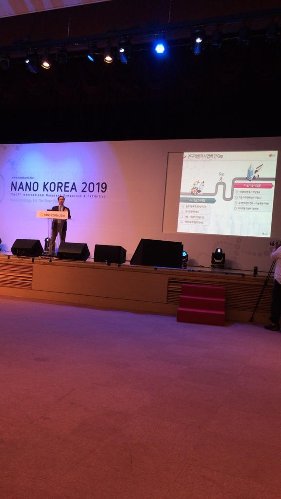
Nano Korea 2019 (Goyang, Korea) - The 17th International Nanotech Symposium and Exhibition were held last week, from July 2nd to July 5th at KINTEX, in Goyang, Korea. Featuring a wide range of companies and countries, the convention showed how quickly the field is growing. As previous visitors, we were eager to see how much progress had been made.
Starting off with the largest of the exhibits, Samsung and LG returned to the exhibition with their stunning displays, with screens spanning 2 meters wide. However, despite the fact that both of these giants of the field showed off their televisions, the focus seemed very different from the year before.
In contrast to last year, where the focus was on the displays themselves, this year, both companies chose to draw attention to the sensors and materials that comprise the displays. This was evident from the fact that although both had several screens to catch the attention of passing viewers, the exhibits themselves showcased different technologies.
Samsung boasted the capabilities of their new sensors, and posted infographics about their work on 2D nanomaterials, such as graphene. They were eager to boast the efficiency and sensitivity of their smallest sensors – more so than the screen as a whole. Perhaps, the most impressive part of their exhibit was their skill in manufacturing sensors on the nano scale – for example, the pixels of the QLED screen were only 10 nm wide, fitting for the exhibit’s name. More so, they showed how their developments in 2D materials (like graphene) are leading to improvements in the aforementioned sensors.
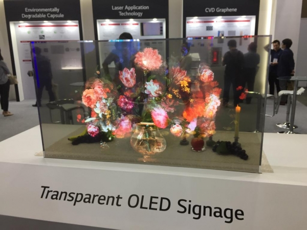
On the other side, LG showed 2 screens – a transparent display, and an extremely thin, vibrant television behind it. To the right, there was information about their OLED materials. However, like Samsung, closer inspection of the information showed that they too had shifted their focus. Graphene was again the star of the show, and LG was eager to show off their progress on it, dubbing it the “New Wonder Material”. Finally, a unique new addition was the “environmentally degradable capsule”, which was a small capsule the size of a common pill, but with fertilizer contained in it. These capsules can be applied like any other fertilizer, but were designed to degrade and release their contents only once they have absorbed water and received UV light. The purpose of this capsule was to allow for a controlled release of fertilizer to crops through the degradation process.
Moving onto products of the centimeter and millimeter scale, we were surprised to see much more real world applications of technologies.
There was a wealth of sensors sold by private firms, such as those to detect vibrations, inertial sensors, or even sensors that used a precision laser to detect the slightest of sounds, even in the ultrasound region.
Many of these sensors and nanomaterials can be utilized in everyday objects – mesh pans, pressure cookers, and air purifiers, to name a few. The variety of nanomaterials used in these everyday objects, as well as their improvements to quality of life, were noteworthy. For example, the usage of nanomaterials as catalysts substantially improved the amount of filtered microdust. Such small changes clearly made enormous differences in terms of efficiency and durability.
All of these innovations have been commercialized, ready to be sold and used in our daily lives, or harnessed on an industrial scale for use by companies or even the military.
The micrometer and nanometer-scaled products featured many different materials as well. In particular, we were pleased to see Mr. Jefford Humes from the Canadian booth again, as he returned with his nanotubes. Last year, he showed us the properties of the nanotubes themselves; this time, however, we were able to have a discussion with him on the creation of the materials. From start to finish – from choosing the material, to reacting it with plasma at an exact temperature and pressure, to dissolving it in a solution with a catalyst, in which the tubes are created – the nanotubes undergo an extensive process in which, if even one measurement is slightly off, “you end up with a completely different product” – in his own words. While this makes extreme precision a prerequisite in order to create a certain carbon tube with the best efficiency, it also opens up doors to many different types of carbon tubes in different applications. Mr. Humes’ job is to consult customers on the different qualities that they want from the carbon tubes, and to find the most optimal conditions at which the requested carbon tubes are of the highest efficiency and quality. “Sometimes it’s a long time frame, but sometimes I can just send them a sample, and they’re happy… but it’s usually a process,” Mr. Humes says.
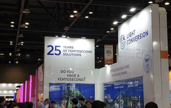
The smallest of the units were reserved for the booths with a pink light – they showcased their laser technology. The lasers focused on the precision and sensitivity that they could offer, and perhaps the one sentence that showed this off the best was the question, “Do you have a femtosecond?”
Although we were relatively new to the field of lasers, we were still impressed by the broad range of applications, whether from machines that could etch on various materials to ones that performed precision work with the shortest of pulses.
Nano Korea 2019 was filled with innovations, as wide as the range of units we saw, from the meter to the femtosecond. Visiting allowed us to see how the trends in technology are shifting to be applied to our daily lives, and, certainly, made us look forward to the future where the smallest of technologies will improve our lives. Indeed, this exhibition made it clear to us that nanomaterials are, indeed, the “building blocks for the future”!
Written by Jacob Kim, Seoul Foreign School (SFS) and Spencer Lee, Seoul Foreign School (SFS)