Samsung Electronics has succeeded in developing world’s first 3-nanometer ultrafine semiconductor process technology.
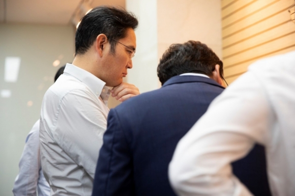
Samsung Electronics Vice Chairman Lee Jae-yong visited Samsung Electronics’ Hwasung business on the 2nd and discussed strategies with presidents of Samsung Electronics’ device solutions division, who is in charge of next-generation semiconductors, after receiving reports on Samsung Electronics’ first 3-nano process technology.
The meeting was attended by Vice Chairman Kim Ki-nam, vice chairman of DS division, President Chung Eun-seung of Foundry Business Department, President Jin Kyo-young of Memory Business Department, President Kang In-yeop of System LSI Business Department, and Vice President Kang Ho-kyu of Semiconductor Research Institute.
3-nano semiconductors, which are applied with GAA (Gate-All-Around), a next-generation technology that can overcome limitations of semiconductor refinement, will reduce area of chips by 35 percent, reduce electricity consumption by 50 percent and speed up processing by about 30 percent compared to 5-nano products that Samsung Electronics recently completed developing processes.
"The past performance does not guarantee future success," said Vice Chairman Lee. "We should make history, not wait. Let`s boldly abandon wrong practices and accidents and explore a new future."